This is the project homepage for wb_switch, a generic, multiplexer based interconnect component for the Wishbone bus, written in VHDL. It includes support for bus arbitration for multiple masters as well as address translation for multiple slaves.
Overview
“Wishbone” is a specification for a parallel bus system, primarily to be used as an on-chip bus to connect several independent logic blocks within one chip design. The Wishbone Bus uses a Master/Slave Concept where only “Master” Components may drive the bus whereas “Slave” components may only use the bus when instructed by a Master component. Also, there may be multiple Master and/or Slave devices present on the bus.
One problem with multiple bus participants is that only one participant may drive the bus at any time. For slave participants, this is relatively easy since slaves may not use the bus when not addressed anyways (but care must be taken to not place two devices on the same bus address). However, multiple bus masters require arbitration so that only the one master to which the bus is granted drives the bus.
There is another problem when designing a shared bus as outlined above inside a single chip, particularily an FPGA: Bus participants which may not drive the bus must neither drive a low, nor a high signal on the bus. Typically, this is done by setting the signal drivers to a “High-Z” state. However, there typically aren’t any Tri-State buffers inside an FPGA, but only the drivers for the I/O Pins are Tri-State capable. Hence, when using this technique on an FPGA, the design tools are required to route the bus signals through the I/O Buffers, which is usually a pessimization with regards to the performance of the design.
wb_switch solves those problems by introducing a switch logic based on multiplexers, a resource that is easily available in FPGAs. That way, each bus participant can be designed as if directly connected to a peer component.
Because the performance of FPGA designs suffers from long unbuffered signal paths, the wb_switch logic organizes its internal components in a pipelined logic. This does not increas the FPGA logic usage, because the required registers are present in the FPGA anyways (it would be a waste not to use them). However, this increases the latency between Wishbone masters and slaves. This doesn’t impact the Wishbone throughput because pipelined transfers can be used.
Architecture
wb_switch consists of four basic blocks: An arbiter, an address translator and two multiplexer components for masters and slaves. Except for the arbiter, the individual blocks implement filters, i.e. each component implements a Wishbone slave interface as well as a Wishbone master interface. Wishbone transfers seen on the slave interface are processed and then re-issued on the master interface. Similar to that, slave responses are forwarded from the master interface implementation to the slave interface implementation. The filters are daisy-chained together, forming a pipeline. Figure 1 below illustrates the architecture.
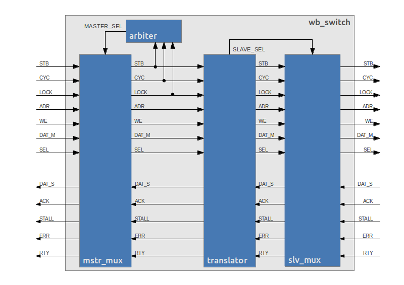
It should be noted that the filters do their processing within one clock cycle. Therefore, both Wishbone classic read/write cycles as well as classic pipelined read/write cycles are supported. As required by the Wishbone specification, the stall signal is not buffered.
Multiplexers
The multiplexer components place a master or slave on the wishbone bus, depending on the select signals driven by the arbiter or the address translator, respectively.
All signals driven by all connected Wishbone Master components are routed into the master multiplexer, and reduced to one set of master-to-slave signals. Respectively, all slave driven signals are reduced to a single set of slave-to-master signals by the slave multiplexer.
Arbiter
The arbiter grants the bus to a master by driving the select signals of the master multiplexer. The current design uses a counter which steps unless the current master has taken the bus, i.e. drives cyc. Hence, once a master has placed a transaction on the bus, the arbiter will not advance to the next master unless the active master releases the bus.
On the other hand, this also means that the master must claim the bus by asserting the cyc until the slave has acknowledged the cycle by asserting either ack, rty or err.
Address Translator
The address translator component is responsible for routing the slave-to-master signals from the currently selected slave back to the active master. Also, it needs to take care that the stb signal is only routed to the targeted slave. Furthermore, the address translator makes sure that no two slaves can respond to the same address on the wishbone bus.
The current design uses the upper bits of the wishbone address to select the slave that is being addressed. While this reduces the address space available for a single slave, it allows all slaves to decode their addresses starting at zero.
Usage
Using the wb_switch component in your VHDL design is as easy as declaring and instantiating any other component. Below is the VHDL entity declaration of the component.
entity wb_switch is
generic (
     -- Width of data bus
     dat_sz      : natural := 8;
     -- Nibble size
     nib_sz      : natural := 8;
     -- Width of address bus
     addr_sz     : natural := 32;
     -- Number of Wishbone Masters (in powers of 2).
     mstr_bits   : natural := 2;
     -- Number of Wishbone Slaves (in powers of 2).
     slv_bits    : natural := 3
);
port (
     clk_i       : in  std_logic;
     rst_i       : in  std_logic;
     --
     -- Whishbone Master Interface
     --
     -- The Signal Directions are inverted as they are coming from/going to
     -- the masters into/from the switch/arbiter logic.
     --
     wb_mstr_cyc_i       : in  std_logic_vector(((2 ** mstr_bits) - 1) downto 0);
     wb_mstr_lock_i      : in  std_logic_vector(((2 ** mstr_bits) - 1) downto 0);
     wb_mstr_stb_i       : in  std_logic_vector(((2 ** mstr_bits) - 1) downto 0);
     wb_mstr_adr_i       : in  std_logic_vector((((2 ** mstr_bits) * addr_sz) - 1) downto 0);
     wb_mstr_we_i        : in  std_logic_vector(((2 ** mstr_bits) - 1) downto 0);
     wb_mstr_dat_i       : in  std_logic_vector((((2 ** mstr_bits) * dat_sz) - 1) downto 0);
     wb_mstr_sel_i       : in  std_logic_vector((((2 ** mstr_bits) * nib_sz) - 1) downto 0);
     wb_mstr_dat_o       : out std_logic_vector((dat_sz - 1) downto 0);
     wb_mstr_ack_o       : out std_logic;
     wb_mstr_stall_o     : out std_logic;
     wb_mstr_err_o       : out std_logic;
     wb_mstr_rty_o       : out std_logic;
     --
     -- Whishbone Slave Interface
     --
     -- The Signal Directions are inverted as they are coming from/going to
     -- the masters into/from the switch/arbiter logic.
     --
     wb_slv_cyc_o       : out std_logic;
     wb_slv_lock_o      : out std_logic;
     wb_slv_stb_o       : out std_logic_vector(((2 ** slv_bits) - 1) downto 0);
     wb_slv_adr_o       : out std_logic_vector((addr_sz - 1) downto 0);
     wb_slv_we_o        : out std_logic;
     wb_slv_dat_o       : out std_logic_vector((dat_sz - 1) downto 0);
     wb_slv_sel_o       : out std_logic_vector((nib_sz - 1) downto 0);
     wb_slv_dat_i       : in  std_logic_vector((((2 ** slv_bits) * dat_sz) - 1) downto 0);
     wb_slv_ack_i       : in  std_logic_vector(((2 ** slv_bits) - 1) downto 0);
     wb_slv_stall_i     : in  std_logic_vector(((2 ** slv_bits) - 1) downto 0);
     wb_slv_err_i       : in  std_logic_vector(((2 ** slv_bits) - 1) downto 0);
     wb_slv_rty_i       : in  std_logic_vector(((2 ** slv_bits) - 1) downto 0)
);
end wb_switch;
The design is customizable through generics, which are described in the following table.
| Generic | Description |
|---|---|
dat_sz | Width of Wishbone data bus. |
nib_sz | Width of the Wishbone sel signal. |
addr_sz | Width of the Wishbone address bus. |
mstr_bits | Determines the number of Wishbone masters that can be connected to the switch. The number of supported Wishbone masters is (2^mstr_bits). |
slv_bits | Determines the number of Wishbone slaves that can be connected to the switch. The number of supported Wishbone slaves is (2^slv_bits). |
Registers
The module does not have any user accessible registers.
Master Ports
The wb_switch module provides several Wishbone master ports through the use of vectors. The table below shows what Wishbone master signals are to be connected to what vector index, based on the assumption that master #n is to be connected.
| Master Signal | Mux Master Port #n |
|---|---|
cyc_o | wb_mstr_cyc_i(n) |
lock_o | wb_mstr_lock_i(n) |
stb_o | wb_mstr_stb_i(n) |
adr_o | wb_mstr_adr_o((((n+1)*adr_sz)-1) downto (n*adr_sz)) |
we_o | wb_mstr_we_i(n) |
dat_o | wb_mstr_dat_i((((n+1)*dat_sz)-1) downto (n*dat_sz)) |
sel_o | wb_mstr_sel_i((((n+1)*nib_sz)-1) downto (n*nib_sz)) |
dat_i | wb_mstr_dat_o((((n+1)*dat_sz)-1) downto (n*dat_sz)) |
ack_i | wb_mstr_ack_o |
rty_i | wb_mstr_rty_o |
err_i | wb_mstr_err_o |
stall_i | wb_mstr_stall_o |
Slave Ports
The wb_switch module provides several Wishbone slave ports through the use of vectors. The table below shows what Wishbone slave signals are to be connected to what vector index, based on the assumption that slave #n is to be connected.
| Slave Signal | Mux Slave Port #n |
|---|---|
cyc_i | wb_slv_cyc_o |
lock_i | wb_slv_lock_o |
stb_i | wb_slv_stb_o(n) |
adr_i | wb_slv_adr_o |
we_i | wb_slv_we_o |
dat_i | wb_slv_dat_o |
sel_i | wb_slv_sel_o |
dat_o | wb_slv_dat_i((((n+1)*dat_sz)-1) downto (n*dat_sz)) |
ack_o | wb_slv_ack_i(n) |
rty_o | wb_slv_rty_i(n) |
err_o | wb_slv_err_i(n) |
stall_o | wb_slv_stall_i(n) |
Download
Below are the links to the VHDL files of the four individual components, as well as the top component which integrates the four.
- Wishbone Switch, wb_switch.vhd
- Master Multiplexer, wb_master_mux.vhd
- Slave Multiplexer, wb_slave_mux.vhd
- Bus Arbiter, wb_arbiter.vhd
- Address Translator, wb_slave_sel.vhd
Links
Here are a few links related to this project.
- Wikipedia Article on the Wishbone Bus.
- The Wishbone Bus Specification, Rev. B4