Linux VNC and Mac OS X Screen Sharing

I’ve found that in order to get x11vnc to work with the Mac OS X built-in VNC client (“Screen Sharing Application”), there options are required when starting the VNC server:

$ x11vnc -display :0 -rfbauth /home/pi/.vnc/passwd -shared -rfbversion 3.3 -forever -bg

The -shared option is key here. Judging by the log on the VNC server, I think Mac OS X will attempt multiple connections.

For what it’s worth, here’s also how to auto-start the VNC server when the user logs into the LXDE desktop. Copy and paste this to ~/.config/autostart/x11vnc.desktop:

[Desktop Entry]
Encoding=UTF-8
Type=Application
Name=VNC
Comment=
Exec=x11vnc -display :0 -rfbauth /home/pi/.vnc/passwd -shared -rfbversion 3.3 -forever -bg
StartupNotify=false
Terminal=false
Hidden=false
Working around KiCAD Printing Issues

I’m having issues printing from KiCAD, specifically Pcbnew, on Ubuntu 15.04. I’ve seen similar things on earlier versions, and also found this bug report. Even though the bug report is closed and I’m using the right wx version, the problem persists for me. So I’ve searched for a workaround.

Luckily, “plotting” from KiCAD works which makes it generate a PostScript file for each layer.

However, I need the “Edge Cuts” layer and the bottom copper layer printed on a single page. The reason is that I’m printing my layouts on transparent film, and I’m using alignment marks on the edge cuts layer to help me tape two prints on top of each other. This increases the opaqueness of my print to a point where it’s usable for me.

So here’s the steps it takes to get my PCB layout to a decent print:

  1. “Plot” the required layers from Pcbnew, leaving a bunch of PostScript files on disk.
  2. Convert the PostScript files to PDF:
    $ for ps in *.ps ; do ps2pdf $ps ; done
    
  3. Use pdftk to generate a single PDF from the relevant layers like this:
    $ pdftk layout-B_Cu.pdf background layout-Edge_Cuts.pdf output layout.pdf
    

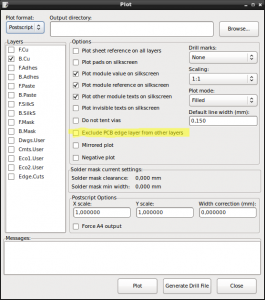
Update: There’s an option to include the “Edge Cuts” layer when plotting. Simply uncheck the “Exclude PCB edge layer from other layers” option as highlighted in the screenshot below.